Difference between revisions of "ADP-KH Adapter Board Data Sheet/zh"
Jump to navigation
Jump to search
(Created page with "English <big><big><big>'''Adapter Board:ADP-KH Data Sheet'''</big></big></big> ==Introduction== The function of ADP-RK is to connect VEYE-MIPI-290/327 and khadas edge board t...") |
|||
| Line 1: | Line 1: | ||
| − | + | [[ADP-KH Adapter Board Data Sheet|English]] | |
| − | |||
| − | == | + | <big><big><big>'''转接板ADP-KH数据手册'''</big></big></big> |
| + | |||
| + | ==产品介绍== | ||
The function of ADP-RK is to connect VEYE-MIPI-290/327 and khadas edge board through FFC. | The function of ADP-RK is to connect VEYE-MIPI-290/327 and khadas edge board through FFC. | ||
{| class="wikitable" | {| class="wikitable" | ||
| Line 20: | Line 21: | ||
[[File:ADP-KH 003 pinlist.jpg|thumb|600x600px|ADP-KH J6 PINLIST]] | [[File:ADP-KH 003 pinlist.jpg|thumb|600x600px|ADP-KH J6 PINLIST]] | ||
| − | == | + | ==转接板接口定义== |
{| class="wikitable" | {| class="wikitable" | ||
| Line 217: | Line 218: | ||
|} | |} | ||
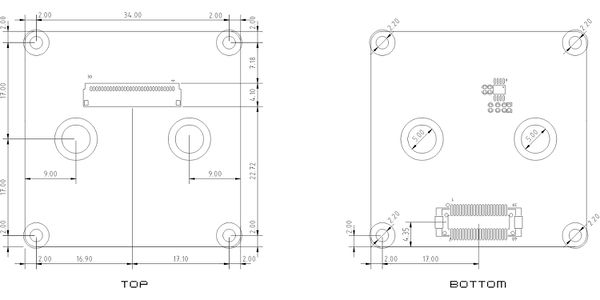
| − | == | + | ==转接板结构尺寸== |
[[File:ADP-KH CAD drawing.jpg|none|thumb|600x600px|ADP-KH CAD / unit:mm]] | [[File:ADP-KH CAD drawing.jpg|none|thumb|600x600px|ADP-KH CAD / unit:mm]] | ||
[[Media:ADP-KH CAD.dwg|Download dwg file here]] | [[Media:ADP-KH CAD.dwg|Download dwg file here]] | ||
Revision as of 06:32, 21 January 2020
转接板ADP-KH数据手册
1 产品介绍
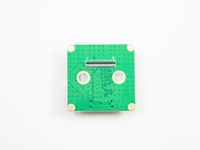
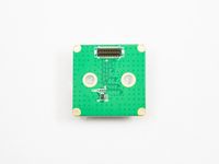
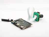
The function of ADP-RK is to connect VEYE-MIPI-290/327 and khadas edge board through FFC.
| PART NUMBER / 型号 | FRONT VIEW / 正面图片 | BACK VIEW / 背面图片 | FFC CABLE/FFC线缆 | SKETCH MAP/示意图 |
| ADK-KH |
2 转接板接口定义
| 1 | VCC3V3 | 2 | VCC3V3 |
| 3 | VCC3V3 | 4 | VCC3V3 |
| 5 | GND | 6 | GND |
| 7 | GND | 8 | GND |
| 9 | MIPI_L0_N | 10 | RESERVE, Not Connected |
| 11 | MIPI_L0_P | 12 | RESERVE, Not Connected |
| 13 | GND | 14 | RESERVE, Not Connected |
| 15 | MIPI_L1_N | 16 | RESERVE, Not Connected |
| 17 | MIPI_L1_P | 18 | RESERVE, Not Connected |
| 19 | GND | 20 | RESERVE, Not Connected |
| 21 | MIPI_CK_N | 22 | SDA(3.3V LEVEL) |
| 23 | MIPI_CK_P | 24 | SCL(3.3V LEVEL) |
| 25 | GND | 26 | GND |
| 27 | RESERVE, Not Connected | 28 | RESERVE, Not Connected |
| 29 | RESERVE, Not Connected | 30 | RESERVE, Not Connected |
| 31 | GND | 32 | RESERVE, Not Connected |
| 33 | RESERVE, Not Connected | 34 | RESERVE, Not Connected |
| 35 | RESERVE, Not Connected | 36 | RESERVE, Not Connected |
| 37 | GND | 38 | RESERVE, Not Connected |
| 39 | RESERVE, Not Connected | 40 | RESERVE, Not Connected |
| 1 | GND |
| 2 | MIPI_L3_N |
| 3 | MIPI_L3_P |
| 4 | GND |
| 5 | MIPI_L2_N |
| 6 | MIPI_L2_P |
| 7 | GND |
| 8 | MIPI_CK_N |
| 9 | MIPI_CK_P |
| 10 | GND |
| 11 | MIPI_L1_N |
| 12 | MIPI_L1_P |
| 13 | GND |
| 14 | MIPI_L0_N |
| 15 | MIPI_L0_P |
| 16 | GND |
| 17 | RESERVE, Not Connected |
| 18 | RESERVE, Not Connected |
| 19 | RESERVE, Not Connected |
| 20 | RESERVE, Not Connected |
| 21 | RESERVE, Not Connected |
| 22 | SCL(1.8V LEVEL) |
| 23 | SDA(1.8V LEVEL) |
| 24 | RESERVE, Not Connected |
| 25 | VCC1V8 |
| 26 | GND |
| 27 | GND |
| 28 | VCC3V3 |
| 29 | VCC3V3 |
| 30 | VCC3V3 |
