Difference between revisions of "VEYE-LVDS-290/327"
Jump to navigation
Jump to search
(Created blank page) |
|||
| (46 intermediate revisions by 3 users not shown) | |||
| Line 1: | Line 1: | ||
| + | [[VEYE-LVDS-290/327/zh|查看中文]] | ||
| + | [[VEYE-LVDS-290/327|<big><big><big><big>VEYE-LVDS-290/VEYE-LVDS-327 Data Sheet</big></big></big></big>]] | ||
| + | |||
| + | ==Introduction== | ||
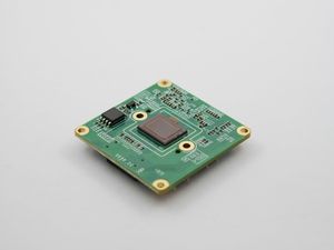
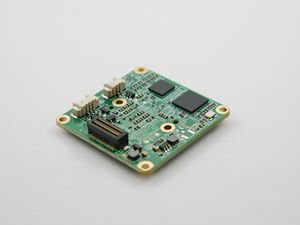
| + | VEYE-LVDS-290/327 is a camera module with excellent low illumination and wide dynamic performance.This module only has 38*38*8mm, which is convenient for integration and can be connected to FPGA boards with adapter board.Suitable for machine vision, intelligent analysis, industrial control, face recognition, ADAS etc... | ||
| + | [[File:VEYE-MIPI-290327-FRONT.jpg|thumb|front]] | ||
| + | [[File:VEYE-MIPI-290327-back.jpg|thumb|back]] | ||
| + | |||
| + | ==Thechnical Detail== | ||
| + | {| class="wikitable" | ||
| + | | colspan="2" |'''Technical Details''' | ||
| + | |- | ||
| + | | colspan="2" |SENSOR | ||
| + | |- | ||
| + | |Sensor | ||
| + | |SONY IMX290LQR-C/IMX327LQR-C STARVIS | ||
| + | |- | ||
| + | |Pixels | ||
| + | |2.07M pixels | ||
| + | |- | ||
| + | |Resolution | ||
| + | |1920*1080 | ||
| + | |- | ||
| + | |Image Size | ||
| + | |Diagonal 6.46 mm (Type 1/2.8) | ||
| + | |- | ||
| + | |Unit Cell Size | ||
| + | |2.9um (H)*2.9um(V) | ||
| + | |- | ||
| + | |[https://www.sony-semicon.co.jp/e/products/IS/security/technology.html '''''SNR1s Value'''''] | ||
| + | |IMX290LQR-C is 0.23lx / IMX327LQR-C is 0.18lx | ||
| + | |- | ||
| + | | colspan="2" |ISP | ||
| + | |- | ||
| + | |Frame Rate | ||
| + | |1080p@25 / 1080p@30fps | ||
| + | |- | ||
| + | |Exposure | ||
| + | |Auto or Manual | ||
| + | |- | ||
| + | |White Balance | ||
| + | |Auto or Manual | ||
| + | |- | ||
| + | |Shutter | ||
| + | |1/25(1/30)s to 1/50,000s | ||
| + | |- | ||
| + | |Slow Shutter | ||
| + | |Support | ||
| + | |- | ||
| + | |Denoising | ||
| + | |2D/3D noise reduction | ||
| + | |- | ||
| + | |Image Setting | ||
| + | |Brightness, Contrast, Sharpness, Saturation,Flip, Mirror | ||
| + | |- | ||
| + | |Image Enhancement | ||
| + | |BLC, DOL-WDR, Defog | ||
| + | |- | ||
| + | |Day/Night Switch | ||
| + | |Manual or IR-CUT filter with external trigger | ||
| + | |- | ||
| + | | colspan="2" |Lens & IR-CUT | ||
| + | |- | ||
| + | |Lens | ||
| + | |Support M12*0.5 or M16*0.5 depend on lens mount | ||
| + | |- | ||
| + | |Lens Mount with IR-CUT | ||
| + | |MTV12 or MTV16 | ||
| + | |- | ||
| + | |Mounting Hole | ||
| + | |2 screw holes with diameter of 2.2mm,20mm Center-to-Center Spacing | ||
| + | |- | ||
| + | | colspan="2" |Interface | ||
| + | |- | ||
| + | |PCB Connector | ||
| + | |BTB connector:BTB050040-F1D | ||
| + | |- | ||
| + | |Communication Interface | ||
| + | |IIC, 3.3VDC | ||
| + | |- | ||
| + | |Video Data Interface | ||
| + | |LVDS:3 Data Lanes, bandwidth:1.5582Gbps | ||
| + | |- | ||
| + | |IR-CUT Control | ||
| + | |IR-CUT motor control, 3.3VDC | ||
| + | |- | ||
| + | |Day/Night External Trigger | ||
| + | |3.3VDC to 12VDC compatibility | ||
| + | |- | ||
| + | | colspan="2" |General | ||
| + | |- | ||
| + | |Operating Conditions | ||
| + | ('''Bare PCB''') | ||
| + | |Performance guarantee temperature:'''-10℃~60℃''', Humidity 95% or less, non-condensing | ||
| + | Operating guarantee temperature: '''-30℃~85℃''', Humidity 95% or less, non-condensing | ||
| + | |- | ||
| + | |Power Supply | ||
| + | |3.3VDC | ||
| + | |- | ||
| + | |Power Consumption | ||
| + | |3.3VDC,1.2W | ||
| + | |- | ||
| + | |Dimension | ||
| + | |38mm*38mm*8mm(not include lens and lens mount) | ||
| + | |} | ||
| + | |||
| + | ==Spectral Sensitivity Characteristics== | ||
| + | {| class="wikitable" | ||
| + | |'''Sensor''' | ||
| + | |'''Spectral Sensitivity''' | ||
| + | |- | ||
| + | |'''IMX290LQR-C''' | ||
| + | |[[File:IMX290LQR-C-SS.jpg|none|thumb|400x400px|IMX290LQR-C Spectral Sensitivity|link=http://wiki.veye.cc/index.php/File:IMX290LQR-C-SS.jpg|alt=]] | ||
| + | |- | ||
| + | |'''IMX327LQR-C''' | ||
| + | |[[File:IMX327LQR-C-SS.jpg|link=http://wiki.veye.cc/index.php/File:IMX327LQR-C-SS.jpg|none|thumb|400x400px|IMX327LQR-C Spectral Sensitivity]] | ||
| + | |}[[File:VEYE-MIPI-290-327接口图.jpg|thumb|VEYE-LVDS-290/327 User Interface|alt=|600x600px]] | ||
| + | ==Connector Pinlist== | ||
| + | {| class="wikitable" | ||
| + | | colspan="6" |'''J5:LVDS Interface''' | ||
| + | |- | ||
| + | |'''Pin NO.''' | ||
| + | |'''NAME''' | ||
| + | |'''Remarks''' | ||
| + | |'''Pin NO.''' | ||
| + | |'''NAME''' | ||
| + | |'''Remarks''' | ||
| + | |- | ||
| + | |1 | ||
| + | |RESERVE | ||
| + | |NC | ||
| + | |2 | ||
| + | |RESERVE | ||
| + | |NC | ||
| + | |- | ||
| + | |3 | ||
| + | |GND | ||
| + | | | ||
| + | |4 | ||
| + | |RESERVE | ||
| + | |NC | ||
| + | |- | ||
| + | |5 | ||
| + | |RESERVE | ||
| + | |NC | ||
| + | |6 | ||
| + | |RESERVE | ||
| + | |NC | ||
| + | |- | ||
| + | |7 | ||
| + | |RESERVE | ||
| + | |NC | ||
| + | |8 | ||
| + | |RESERVE | ||
| + | |NC | ||
| + | |- | ||
| + | |9 | ||
| + | |GND | ||
| + | | | ||
| + | |10 | ||
| + | |GND | ||
| + | | | ||
| + | |- | ||
| + | |11 | ||
| + | |LVDS_L2_P | ||
| + | | | ||
| + | |12 | ||
| + | |RESERVE | ||
| + | |NC | ||
| + | |- | ||
| + | |13 | ||
| + | |LVDS_L2_N | ||
| + | | | ||
| + | |14 | ||
| + | |RESERVE | ||
| + | |NC | ||
| + | |- | ||
| + | |15 | ||
| + | |GND | ||
| + | | | ||
| + | |16 | ||
| + | |GND | ||
| + | | | ||
| + | |- | ||
| + | |17 | ||
| + | |LVDS_CK_P | ||
| + | | | ||
| + | |18 | ||
| + | |SCL | ||
| + | |3.3V Level | ||
| + | |- | ||
| + | |19 | ||
| + | |LVDS_CK_N | ||
| + | | | ||
| + | |20 | ||
| + | |SDA | ||
| + | |3.3V Level | ||
| + | |- | ||
| + | |21 | ||
| + | |GND | ||
| + | | | ||
| + | |22 | ||
| + | |RESERVE | ||
| + | |NC | ||
| + | |- | ||
| + | |23 | ||
| + | |LVDS_L1_P | ||
| + | | | ||
| + | |24 | ||
| + | |RESERVE | ||
| + | |NC | ||
| + | |- | ||
| + | |25 | ||
| + | |LVDS_L1_N | ||
| + | | | ||
| + | |26 | ||
| + | |RESERVE | ||
| + | |NC | ||
| + | |- | ||
| + | |27 | ||
| + | |GND | ||
| + | | | ||
| + | |28 | ||
| + | |RESERVE | ||
| + | |NC | ||
| + | |- | ||
| + | |29 | ||
| + | |LVDS_L0_P | ||
| + | | | ||
| + | |30 | ||
| + | |RESERVE | ||
| + | |NC | ||
| + | |- | ||
| + | |31 | ||
| + | |LVDS_L0_N | ||
| + | | | ||
| + | |32 | ||
| + | |RESERVE | ||
| + | |NC | ||
| + | |- | ||
| + | |33 | ||
| + | |GND | ||
| + | | | ||
| + | |34 | ||
| + | |GND | ||
| + | | | ||
| + | |- | ||
| + | |35 | ||
| + | |GND | ||
| + | | | ||
| + | |36 | ||
| + | |GND | ||
| + | | | ||
| + | |- | ||
| + | |37 | ||
| + | |VCC3V3 | ||
| + | |PWR IN | ||
| + | |38 | ||
| + | |VCC3V3 | ||
| + | |PWR IN | ||
| + | |- | ||
| + | |39 | ||
| + | |VCC3V3 | ||
| + | |PWR IN | ||
| + | |40 | ||
| + | |VCC3V3 | ||
| + | |PWR IN | ||
| + | |} | ||
| + | {| class="wikitable" | ||
| + | | colspan="3" |'''J3 : Day / Night External Trigger''' | ||
| + | |- | ||
| + | |'''Pin NO.''' | ||
| + | |'''NAME''' | ||
| + | |'''Remarks''' | ||
| + | |- | ||
| + | |1 | ||
| + | |Day&Night Signal In | ||
| + | |INPUT,Active High(Image to MONO),3.3VDC to 12VDC compatibility | ||
| + | |- | ||
| + | |2 | ||
| + | |GND | ||
| + | | | ||
| + | |- | ||
| + | |3 | ||
| + | |NC | ||
| + | | | ||
| + | |} | ||
| + | {| class="wikitable" | ||
| + | | colspan="3" |'''J4 : IRCUT Control''' | ||
| + | |- | ||
| + | |'''Pin NO.''' | ||
| + | |'''NAME''' | ||
| + | |'''Remarks''' | ||
| + | |- | ||
| + | |1 | ||
| + | |IRCUT1 | ||
| + | | | ||
| + | |- | ||
| + | |2 | ||
| + | |IRCUT2 | ||
| + | | | ||
| + | |} | ||
| + | {| class="wikitable" | ||
| + | | colspan="5" |'''J4 : IRCUT Control Functional specifications''' | ||
| + | |- | ||
| + | |'''MODE''' | ||
| + | |'''PIN''' | ||
| + | |'''Signal polarity''' | ||
| + | |'''Image type''' | ||
| + | |'''Filter position''' | ||
| + | |- | ||
| + | | rowspan="2" |Mode 1 | ||
| + | |IRCUT1 | ||
| + | | + | ||
| + | | rowspan="2" |color | ||
| + | | rowspan="2" |Infrared cutoff | ||
| + | |- | ||
| + | |IRCUT2 | ||
| + | | - | ||
| + | |- | ||
| + | | rowspan="2" |Mode 2 | ||
| + | |IRCUT1 | ||
| + | | - | ||
| + | | rowspan="2" |mono | ||
| + | | rowspan="2" |Full wavelength pass | ||
| + | |- | ||
| + | |IRCUT2 | ||
| + | | + | ||
| + | |} | ||
| + | |||
| + | ==Board Dimension== | ||
| + | [[File:VEYE-MIPI-290-327 CAD drawing.jpg|thumb|VEYE-LVDS-290/327 CAD drawing|alt=|none|600x600px]] | ||
| + | [[Media:VEYE-MIPI-327 CAD.dwg|Download dwg file here]] | ||
| + | == PCBA 3D STP File == | ||
| + | [[Media:3D VEYE-LVDS-327.zip|download 3D STP file]] | ||
| + | |||
| + | ==Imaging Effect== | ||
| + | |||
| + | ==CPU boards== | ||
| + | |||
| + | *Demo for FPGA usage | ||
| + | |||
| + | We provide a demo for FPGA usage,check link [https://github.com/veyeimaging/fpga here]. | ||
| + | |||
| + | ==Resources== | ||
| + | ==Update Log== | ||
Latest revision as of 04:01, 30 December 2021
VEYE-LVDS-290/VEYE-LVDS-327 Data Sheet
1 Introduction
VEYE-LVDS-290/327 is a camera module with excellent low illumination and wide dynamic performance.This module only has 38*38*8mm, which is convenient for integration and can be connected to FPGA boards with adapter board.Suitable for machine vision, intelligent analysis, industrial control, face recognition, ADAS etc...
2 Thechnical Detail
| Technical Details | |
| SENSOR | |
| Sensor | SONY IMX290LQR-C/IMX327LQR-C STARVIS |
| Pixels | 2.07M pixels |
| Resolution | 1920*1080 |
| Image Size | Diagonal 6.46 mm (Type 1/2.8) |
| Unit Cell Size | 2.9um (H)*2.9um(V) |
| SNR1s Value | IMX290LQR-C is 0.23lx / IMX327LQR-C is 0.18lx |
| ISP | |
| Frame Rate | 1080p@25 / 1080p@30fps |
| Exposure | Auto or Manual |
| White Balance | Auto or Manual |
| Shutter | 1/25(1/30)s to 1/50,000s |
| Slow Shutter | Support |
| Denoising | 2D/3D noise reduction |
| Image Setting | Brightness, Contrast, Sharpness, Saturation,Flip, Mirror |
| Image Enhancement | BLC, DOL-WDR, Defog |
| Day/Night Switch | Manual or IR-CUT filter with external trigger |
| Lens & IR-CUT | |
| Lens | Support M12*0.5 or M16*0.5 depend on lens mount |
| Lens Mount with IR-CUT | MTV12 or MTV16 |
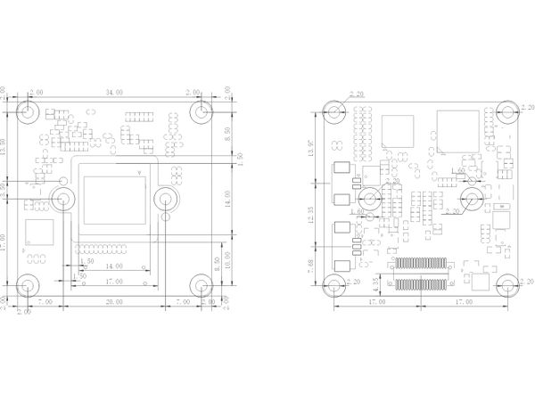
| Mounting Hole | 2 screw holes with diameter of 2.2mm,20mm Center-to-Center Spacing |
| Interface | |
| PCB Connector | BTB connector:BTB050040-F1D |
| Communication Interface | IIC, 3.3VDC |
| Video Data Interface | LVDS:3 Data Lanes, bandwidth:1.5582Gbps |
| IR-CUT Control | IR-CUT motor control, 3.3VDC |
| Day/Night External Trigger | 3.3VDC to 12VDC compatibility |
| General | |
| Operating Conditions
(Bare PCB) |
Performance guarantee temperature:-10℃~60℃, Humidity 95% or less, non-condensing
Operating guarantee temperature: -30℃~85℃, Humidity 95% or less, non-condensing |
| Power Supply | 3.3VDC |
| Power Consumption | 3.3VDC,1.2W |
| Dimension | 38mm*38mm*8mm(not include lens and lens mount) |
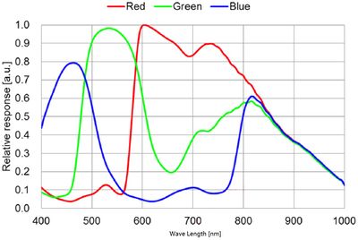
3 Spectral Sensitivity Characteristics
| Sensor | Spectral Sensitivity |
| IMX290LQR-C | |
| IMX327LQR-C |
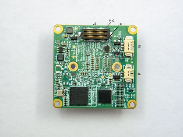
4 Connector Pinlist
| J5:LVDS Interface | |||||
| Pin NO. | NAME | Remarks | Pin NO. | NAME | Remarks |
| 1 | RESERVE | NC | 2 | RESERVE | NC |
| 3 | GND | 4 | RESERVE | NC | |
| 5 | RESERVE | NC | 6 | RESERVE | NC |
| 7 | RESERVE | NC | 8 | RESERVE | NC |
| 9 | GND | 10 | GND | ||
| 11 | LVDS_L2_P | 12 | RESERVE | NC | |
| 13 | LVDS_L2_N | 14 | RESERVE | NC | |
| 15 | GND | 16 | GND | ||
| 17 | LVDS_CK_P | 18 | SCL | 3.3V Level | |
| 19 | LVDS_CK_N | 20 | SDA | 3.3V Level | |
| 21 | GND | 22 | RESERVE | NC | |
| 23 | LVDS_L1_P | 24 | RESERVE | NC | |
| 25 | LVDS_L1_N | 26 | RESERVE | NC | |
| 27 | GND | 28 | RESERVE | NC | |
| 29 | LVDS_L0_P | 30 | RESERVE | NC | |
| 31 | LVDS_L0_N | 32 | RESERVE | NC | |
| 33 | GND | 34 | GND | ||
| 35 | GND | 36 | GND | ||
| 37 | VCC3V3 | PWR IN | 38 | VCC3V3 | PWR IN |
| 39 | VCC3V3 | PWR IN | 40 | VCC3V3 | PWR IN |
| J3 : Day / Night External Trigger | ||
| Pin NO. | NAME | Remarks |
| 1 | Day&Night Signal In | INPUT,Active High(Image to MONO),3.3VDC to 12VDC compatibility |
| 2 | GND | |
| 3 | NC | |
| J4 : IRCUT Control | ||
| Pin NO. | NAME | Remarks |
| 1 | IRCUT1 | |
| 2 | IRCUT2 | |
| J4 : IRCUT Control Functional specifications | ||||
| MODE | PIN | Signal polarity | Image type | Filter position |
| Mode 1 | IRCUT1 | + | color | Infrared cutoff |
| IRCUT2 | - | |||
| Mode 2 | IRCUT1 | - | mono | Full wavelength pass |
| IRCUT2 | + | |||
5 Board Dimension
6 PCBA 3D STP File
7 Imaging Effect
8 CPU boards
- Demo for FPGA usage
We provide a demo for FPGA usage,check link here.
