Difference between revisions of "FPD-LINK3-TX Data Sheet index"
Jump to navigation
Jump to search
| (4 intermediate revisions by the same user not shown) | |||
| Line 19: | Line 19: | ||
|- | |- | ||
|IC PART NO. | |IC PART NO. | ||
| − | |[https://www.ti.com/product/DS90UB953-Q1 DS90UB953-Q1] | + | |[https://www.ti.com/product/DS90UB953-Q1 DS90UB953-Q1] / [https://www.ti.com/product/TSER953 TSER953RHBT] |
|- | |- | ||
|Function | |Function | ||
| Line 28: | Line 28: | ||
|- | |- | ||
|Output Compatibility | |Output Compatibility | ||
| − | |FPD-Link III LVDS | + | |[https://www.ti.com/interface/high-speed-serdes/fpd-link-serdes/overview.html FPD-Link III LVDS] / [https://www.ti.com/interface/high-speed-serdes/v3link-serdes/overview.html V3Link SerDes] |
|- | |- | ||
|'''Interface''' | |'''Interface''' | ||
| Line 73: | Line 73: | ||
|Operating Conditions | |Operating Conditions | ||
('''Bare PCB''') | ('''Bare PCB''') | ||
| − | |Operating guarantee temperature:'''- | + | |Operating guarantee temperature:'''-20℃~85℃''', Humidity 95% or less, non-condensing |
|- | |- | ||
|POC DC Power Input | |POC DC Power Input | ||
| Line 87: | Line 87: | ||
==Board Pinlist(接口和引脚说明)== | ==Board Pinlist(接口和引脚说明)== | ||
{| class="wikitable" | {| class="wikitable" | ||
| − | | colspan="3" |'''J1''' | + | | colspan="3" |'''J1:''' |
| + | '''Connect to CS-MIPI-SC132's J7''' | ||
| + | |||
| + | '''Connect to CS-MIPI-IMX307's J7''' | ||
|- | |- | ||
|'''<small>Pin NO.(引脚号)</small>''' | |'''<small>Pin NO.(引脚号)</small>''' | ||
| Line 95: | Line 98: | ||
|1 | |1 | ||
|MPIO0 | |MPIO0 | ||
| − | | | + | |3.3V Level |
|- | |- | ||
|2 | |2 | ||
| Line 103: | Line 106: | ||
|3 | |3 | ||
|MPIO1 | |MPIO1 | ||
| − | | | + | |3.3V Level |
|} | |} | ||
{| class="wikitable" | {| class="wikitable" | ||
| Line 114: | Line 117: | ||
|1 | |1 | ||
|MPIO2 | |MPIO2 | ||
| − | | | + | |3.3V Level |
|- | |- | ||
|2 | |2 | ||
| Line 122: | Line 125: | ||
|3 | |3 | ||
|MPIO3 | |MPIO3 | ||
| − | | | + | |3.3V Level |
|} | |} | ||
{| class="wikitable" | {| class="wikitable" | ||
| Line 399: | Line 402: | ||
|11 | |11 | ||
|MPIO1 | |MPIO1 | ||
| − | | | + | |3.3V Level |
|- | |- | ||
|12 | |12 | ||
|MPIO0 | |MPIO0 | ||
| − | | | + | |3.3V Level |
|- | |- | ||
|13 | |13 | ||
Latest revision as of 03:22, 9 October 2022
FPD-LINK3-TX Data Sheet (FPD-LINK3-TX数据手册)
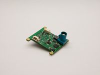
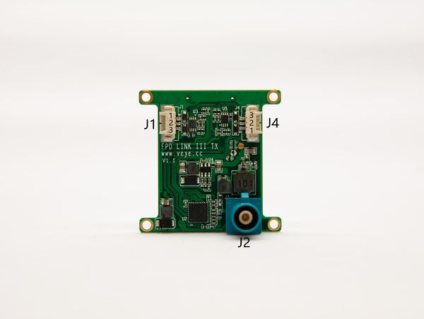
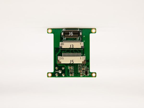
1 Product Picture(产品图片)
| PART NUMBER / 型号 | FRONT VIEW / 正面图片 | BACK VIEW / 背面图片 |
| FPD-LINK3-TX |
2 Thechnical Detail (技术规格)
| Thechnical Detail (技术规格) | |
| 2 MP MIPI® CSI-2 FPD-Link III serializer | |
| IC PART NO. | DS90UB953-Q1 / TSER953RHBT |
| Function | Serializer |
| Input Compatibility | MIPI CSI-2 |
| Output Compatibility | FPD-Link III LVDS / V3Link SerDes |
| Interface | |
| MIPI INPUT | MIPI CSI-2 2lane (800Mbsp/lane max), J5 J6 Support
MIPI CSI-2 4lane (800Mbsp/lane max), J3 Support |
| MIPI INPUT Connector | FFC socket(J3 J5),B2B Connector(J6) |
| LVDS OUTPUT | FPD-Link III LVDS (4Gbps data rate) |
| LVDS OUTPUT Connector | FAKRA Z Compatibility |
| MPIO | Up to 4 Multi-function IO |
| Device Functional Modes | |
| Clocking Mode | Synchronous Mode, FPD-Link III Clock reference derived from deserializer |
| FPD-Link III Operating Mode | CSI-2 Mode |
| Forward Channel Mode | Synchronous Mode |
| Back Channel Mode | Synchronous Mode |
| FPD-Link Line Rate | 4.0 Gbps (Link with FPD-LINK3-2RX) |
| Back Channel Rate | 50 Mbps (Link with FPD-LINK3-2RX) |
| General | |
| Operating Conditions
(Bare PCB) |
Operating guarantee temperature:-20℃~85℃, Humidity 95% or less, non-condensing |
| POC DC Power Input | DC 9-15V (J2) |
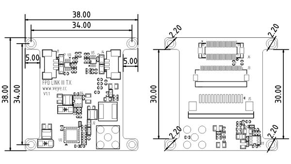
| Dimension | 38mm*38mm |
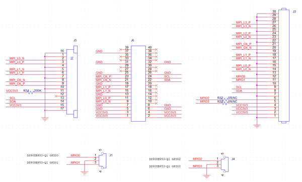
3 Board Pinlist(接口和引脚说明)
| J1:
Connect to CS-MIPI-SC132's J7 Connect to CS-MIPI-IMX307's J7 | ||
| Pin NO.(引脚号) | NAME(名称) | Remarks(说明) |
| 1 | MPIO0 | 3.3V Level |
| 2 | GND | |
| 3 | MPIO1 | 3.3V Level |
| J4 | ||
| Pin NO.(引脚号) | NAME(名称) | Remarks(说明) |
| 1 | MPIO2 | 3.3V Level |
| 2 | GND | |
| 3 | MPIO3 | 3.3V Level |
| J2:POC interface(POC接口) | |
| Connector(接插件) | Interface Definition(接口定义) |
| FAKRA Z | |
| J5 : Connect to CS-MIPI-IMX307's J8 (与CS-MIPI-IMX307 J8互联) | ||
| Pin NO.(引脚号) | NAME(名称) | Remarks(说明) |
| 1 | GND | |
| 2 | MIPI_L0_N | |
| 3 | MIPI_L0_P | |
| 4 | GND | |
| 5 | MIPI_L1_N | |
| 6 | MIPI_L1_P | |
| 7 | GND | |
| 8 | MIPI_CK_N | |
| 9 | MIPI_CK_P | |
| 10 | GND | |
| 11 | RESERVE | NC |
| 12 | RESERVE | NC |
| 13 | SCL | 3.3V Level |
| 14 | SDA | 3.3V Level |
| 15 | VCC3V3 | PWR OUT |
| J6:Connect to VEYE-MIPI-327's J5 (与VEYE-MIPI-327 J5互联) | |||||
| Pin NO.(引脚号) | NAME(名称) | Remarks(说明) | Pin NO.(引脚号) | NAME(名称) | Remarks(说明) |
| 1 | VCC3V3 | PWR OUT | 2 | VCC3V3 | PWR OUT |
| 3 | VCC3V3 | PWR OUT | 4 | VCC3V3 | PWR OUT |
| 5 | GND | 6 | GND | ||
| 7 | GND | 8 | GND | ||
| 9 | MIPI_L0_N | 10 | NC | ||
| 11 | MIPI_L0_P | 12 | NC | ||
| 13 | GND | 14 | NC | ||
| 15 | MIPI_L1_N | 16 | NC | ||
| 17 | MIPI_L1_P | 18 | NC | ||
| 19 | GND | 20 | NC | ||
| 21 | MIPI_CK_N | 22 | SDA | 3.3V LEVEL | |
| 23 | MIPI_CK_P | 24 | SCL | 3.3V LEVEL | |
| 25 | GND | 26 | GND | ||
| 27 | NC | 28 | NC | ||
| 29 | NC | 30 | NC | ||
| 31 | GND | 32 | GND | ||
| 33 | NC | 34 | NC | ||
| 35 | NC | 36 | NC | ||
| 37 | GND | 38 | NC | ||
| 39 | NC | 40 | NC | ||
| J3: RESERVE (预留) | ||
| Pin NO.(引脚号) | NAME(名称) | Remarks(说明) |
| 1 | GND | |
| 2 | VCC3V3 | PWR OUT |
| 3 | VCC3V3 | PWR OUT |
| 4 | VCC3V3 | PWR OUT |
| 5 | MPIO3 | |
| 6 | MPIO2 | |
| 7 | GND | |
| 8 | SDA | 3.3V LEVEL |
| 9 | SCL | 3.3V LEVEL |
| 10 | GND | |
| 11 | MPIO1 | 3.3V Level |
| 12 | MPIO0 | 3.3V Level |
| 13 | GND | |
| 14 | MIPI_L0_N | |
| 15 | MIPI_L0_P | |
| 16 | GND | |
| 17 | MIPI_L1_N | |
| 18 | MIPI_L1_P | |
| 19 | GND | |
| 20 | MIPI_CK_N | |
| 21 | MIPI_CK_P | |
| 22 | GND | |
| 23 | MIPI_L2_N | |
| 24 | MIPI_L2_P | |
| 25 | GND | |
| 26 | MIPI_L3_N | |
| 27 | MIPI_L3_P | |
| 28 | GND | |
