Difference between revisions of "Mini Adapter Board"
Jump to navigation
Jump to search
| (5 intermediate revisions by the same user not shown) | |||
| Line 1: | Line 1: | ||
| − | [ | + | [[Mini Adapter Board/zh|查看中文]] |
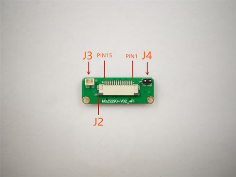
[[File:VeyeRaspberryPi Base T rock.jpg|thumb|485x485px|connector position(front)]] | [[File:VeyeRaspberryPi Base T rock.jpg|thumb|485x485px|connector position(front)]] | ||
'''<big><big><big>ADP-B Mini Adapter Board for Raspberry Pi Data Sheet</big></big></big>''' | '''<big><big><big>ADP-B Mini Adapter Board for Raspberry Pi Data Sheet</big></big></big>''' | ||
==Introduction== | ==Introduction== | ||
| − | Mini Adapter Board connect the [ | + | Mini Adapter Board connect the [[VEYE MIPI 290/327 for Raspberry Pi/zh|Raspberry Pi]]: |
Connect J2 interface and CSI-2 interface on Raspberry Pi with 1.00mm15pin pitch FFC cable(TypeB). | Connect J2 interface and CSI-2 interface on Raspberry Pi with 1.00mm15pin pitch FFC cable(TypeB). | ||
==Adapter Board Diagram,Layout== | ==Adapter Board Diagram,Layout== | ||
| − | + | ||
{| class="wikitable" | {| class="wikitable" | ||
| colspan="3" |'''J2''' | | colspan="3" |'''J2''' | ||
|- | |- | ||
| − | |''' | + | |'''Pin NO.''' |
| − | |''' | + | |'''NAME''' |
| − | |''' | + | |'''Remarks''' |
|- | |- | ||
|1 | |1 | ||
| Line 85: | Line 85: | ||
| colspan="3" |'''J3''' | | colspan="3" |'''J3''' | ||
|- | |- | ||
| − | |''' | + | |'''Pin NO.''' |
| − | |''' | + | |'''NAME''' |
| − | |''' | + | |'''Remarks''' |
|- | |- | ||
|1 | |1 | ||
| − | | | + | |VCC5V |
| − | | | + | |PWR IN |
|- | |- | ||
|2 | |2 | ||
|GND | |GND | ||
| | | | ||
| − | |} | + | |} |
{| class="wikitable" | {| class="wikitable" | ||
| colspan="3" |'''J4''' | | colspan="3" |'''J4''' | ||
|- | |- | ||
| − | |''' | + | |'''Pin NO.''' |
| − | |''' | + | |'''NAME''' |
| − | |''' | + | |'''Remarks''' |
|- | |- | ||
|1 | |1 | ||
| − | | | + | |VCC5V |
| − | | | + | |PWR IN |
|- | |- | ||
|2 | |2 | ||
|GND | |GND | ||
| | | | ||
| − | |} | + | |} |
{| class="wikitable" | {| class="wikitable" | ||
| colspan="6" |'''J1''' | | colspan="6" |'''J1''' | ||
|- | |- | ||
| − | |''' | + | |'''Pin NO.''' |
| − | |''' | + | |'''NAME''' |
| − | |''' | + | |'''Remarks''' |
| − | |''' | + | |'''Pin NO.''' |
| − | |''' | + | |'''NAME''' |
| − | |''' | + | |'''Remarks''' |
|- | |- | ||
|1 | |1 | ||
| Line 182: | Line 182: | ||
| | | | ||
|18 | |18 | ||
| − | | | + | |SCL |
|3.3V Level | |3.3V Level | ||
|- | |- | ||
| Line 189: | Line 189: | ||
| | | | ||
|20 | |20 | ||
| − | | | + | |SDA |
|3.3V Level | |3.3V Level | ||
|- | |- | ||
| Line 263: | Line 263: | ||
|} | |} | ||
| − | == Board Diagram == | + | ==Board Diagram== |
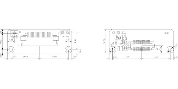
[[File:ADP-B CAD drawing.jpg|none|thumb|600x600px| ADP-B CAD drawing unit:mm|alt=]] | [[File:ADP-B CAD drawing.jpg|none|thumb|600x600px| ADP-B CAD drawing unit:mm|alt=]] | ||
[[Media:ADP-B CAD.dwg|Download dwg file here]] | [[Media:ADP-B CAD.dwg|Download dwg file here]] | ||
Latest revision as of 09:56, 30 January 2026
ADP-B Mini Adapter Board for Raspberry Pi Data Sheet
1 Introduction
Mini Adapter Board connect the Raspberry Pi:
Connect J2 interface and CSI-2 interface on Raspberry Pi with 1.00mm15pin pitch FFC cable(TypeB).
2 Adapter Board Diagram,Layout
| J2 | ||
| Pin NO. | NAME | Remarks |
| 1 | GND | |
| 2 | MIPI_L0_N | |
| 3 | MIPI_L0_P | |
| 4 | GND | |
| 5 | MIPI_L1_N | |
| 6 | MIPI_L1_P | |
| 7 | GND | |
| 8 | MIPI_CK_N | |
| 9 | MIPI_CK_P | |
| 10 | GND | |
| 11 | RESERVE | NC |
| 12 | RESERVE | NC |
| 13 | SCL | 3.3V Level |
| 14 | SDA | 3.3V Level |
| 15 | RESERVE | NC |
| J3 | ||
| Pin NO. | NAME | Remarks |
| 1 | VCC5V | PWR IN |
| 2 | GND | |
| J4 | ||
| Pin NO. | NAME | Remarks |
| 1 | VCC5V | PWR IN |
| 2 | GND | |
| J1 | |||||
| Pin NO. | NAME | Remarks | Pin NO. | NAME | Remarks |
| 1 | RESERVE | NC | 2 | RESERVE | NC |
| 3 | GND | 4 | RESERVE | NC | |
| 5 | RESERVE | NC | 6 | RESERVE | NC |
| 7 | RESERVE | NC | 8 | RESERVE | NC |
| 9 | GND | 10 | GND | ||
| 11 | RESERVE | NC | 12 | RESERVE | NC |
| 13 | RESERVE | NC | 14 | RESERVE | NC |
| 15 | GND | 16 | GND | ||
| 17 | MIPI_CK_P | 18 | SCL | 3.3V Level | |
| 19 | MIPI_CK_N | 20 | SDA | 3.3V Level | |
| 21 | GND | 22 | RESERVE | NC | |
| 23 | MIPI_L1_P | 24 | RESERVE | NC | |
| 25 | MIPI_L1_N | 26 | RESERVE | NC | |
| 27 | GND | 28 | RESERVE | NC | |
| 29 | MIPI_L0_P | 30 | RESERVE | NC | |
| 31 | MIPI_L0_N | 32 | RESERVE | NC | |
| 33 | GND | 34 | GND | ||
| 35 | GND | 36 | GND | ||
| 37 | VCC3V3 | 38 | VCC3V3 | ||
| 39 | VCC3V3 | 40 | VCC3V3 | ||

