Difference between revisions of "FPD-LINK3-2RX Data Sheet index"
Jump to navigation
Jump to search
| (9 intermediate revisions by one other user not shown) | |||
| Line 7: | Line 7: | ||
|'''BACK VIEW / 背面图片''' | |'''BACK VIEW / 背面图片''' | ||
|- | |- | ||
| − | |'''FPD-LINK3- | + | |'''FPD-LINK3-2RX''' |
|[[File:FPD-LINK3-2RX 03.jpg|alt=|center|thumb|200x200px]] | |[[File:FPD-LINK3-2RX 03.jpg|alt=|center|thumb|200x200px]] | ||
|[[File:FPD-LINK3-2RX 04.jpg|alt=|center|thumb|200x200px]] | |[[File:FPD-LINK3-2RX 04.jpg|alt=|center|thumb|200x200px]] | ||
| Line 20: | Line 20: | ||
|- | |- | ||
|IC PART NO. | |IC PART NO. | ||
| − | |[https://www.ti.com/product/DS90UB954-Q1?keyMatch=DS90UB954-Q1&tisearch=Search-EN-everything DS90UB954-Q1] | + | |[https://www.ti.com/product/DS90UB954-Q1?keyMatch=DS90UB954-Q1&tisearch=Search-EN-everything DS90UB954-Q1] / [https://www.ti.com/product/TDES954 TDES954RGZT] |
|- | |- | ||
|Function | |Function | ||
| Line 26: | Line 26: | ||
|- | |- | ||
|Input Compatibility | |Input Compatibility | ||
| − | |FPD-Link III LVDS | + | |[https://www.ti.com/interface/high-speed-serdes/fpd-link-serdes/overview.html FPD-Link III LVDS] / [https://www.ti.com/interface/high-speed-serdes/v3link-serdes/overview.html V3Link SerDes] |
|- | |- | ||
|Output Compatibility | |Output Compatibility | ||
| Line 41: | Line 41: | ||
|- | |- | ||
|MIPI Output Connector | |MIPI Output Connector | ||
| − | |FFC socket(J7 J9) | + | |FFC socket(J7 / J9) |
|- | |- | ||
|LVDS Input | |LVDS Input | ||
| Line 47: | Line 47: | ||
|- | |- | ||
|LVDS Input Connector | |LVDS Input Connector | ||
| − | |FAKRA Z Compatibility * 2 | + | |FAKRA Z Compatibility * 2, '''J3(Port 0), J4(Port 1)''' |
|- | |- | ||
|MPIO | |MPIO | ||
| Line 54: | Line 54: | ||
| colspan="2" |'''Device Functional Modes''' | | colspan="2" |'''Device Functional Modes''' | ||
|- | |- | ||
| − | |FPD-Link III Operating | + | |FPD-Link III Operating Mode |
|CSI-2 Mode (DS90UB953-Q1 and DS90UB935-Q1 compatible) | |CSI-2 Mode (DS90UB953-Q1 and DS90UB935-Q1 compatible) | ||
|- | |- | ||
| − | |Forward Channel | + | |Forward Channel Mode |
|Synchronous Mode | |Synchronous Mode | ||
|- | |- | ||
| Line 73: | Line 73: | ||
|Operating Conditions | |Operating Conditions | ||
('''Bare PCB''') | ('''Bare PCB''') | ||
| − | |Operating guarantee temperature:'''- | + | |Operating guarantee temperature:'''-20℃~85℃''', Humidity 95% or less, non-condensing |
|- | |- | ||
|DC Power Supply | |DC Power Supply | ||
| Line 109: | Line 109: | ||
|'''Interface Definition(接口定义)''' | |'''Interface Definition(接口定义)''' | ||
|- | |- | ||
| − | |DC | + | |DC JACK |
|[[File:Polarity diagram.png|center|thumb|200x200px|'''+:12VIN / -:GND'''|alt=]] | |[[File:Polarity diagram.png|center|thumb|200x200px|'''+:12VIN / -:GND'''|alt=]] | ||
|} | |} | ||
{| class="wikitable" | {| class="wikitable" | ||
| colspan="2" |'''J3 J4: POC interface(POC接口)''' | | colspan="2" |'''J3 J4: POC interface(POC接口)''' | ||
| + | '''J3(Port 0 / P0)''' | ||
| + | |||
| + | '''J4(Port 1 / P1)''' | ||
|- | |- | ||
|'''Connector(接插件)''' | |'''Connector(接插件)''' | ||
| Line 130: | Line 133: | ||
|1 | |1 | ||
|MPIO4 | |MPIO4 | ||
| − | | | + | |3.3V LEVEL |
|- | |- | ||
|2 | |2 | ||
|MPIO5 | |MPIO5 | ||
| − | | | + | |3.3V LEVEL |
|- | |- | ||
|3 | |3 | ||
|MPIO6 | |MPIO6 | ||
| − | | | + | |3.3V LEVEL |
|- | |- | ||
|4 | |4 | ||
| Line 157: | Line 160: | ||
|1 | |1 | ||
|MPIO0 | |MPIO0 | ||
| − | | | + | |3.3V LEVEL |
|1 | |1 | ||
|MPIO2 | |MPIO2 | ||
| − | | | + | |3.3V LEVEL |
|- | |- | ||
|2 | |2 | ||
| Line 171: | Line 174: | ||
|3 | |3 | ||
|MPIO1 | |MPIO1 | ||
| − | | | + | |3.3V LEVEL |
|3 | |3 | ||
|MPIO3 | |MPIO3 | ||
| − | | | + | |3.3V LEVEL |
|} | |} | ||
{| class="wikitable" | {| class="wikitable" | ||
| Line 252: | Line 255: | ||
|- | |- | ||
|18 | |18 | ||
| − | | | + | |MPIO1 |
| | | | ||
|- | |- | ||
| Line 273: | Line 276: | ||
|23 | |23 | ||
|MPIO2 | |MPIO2 | ||
| − | | | + | |3.3V LEVEL |
|- | |- | ||
|24 | |24 | ||
|MPIO3 | |MPIO3 | ||
| − | | | + | |3.3V LEVEL |
|- | |- | ||
|25 | |25 | ||
| Line 415: | Line 418: | ||
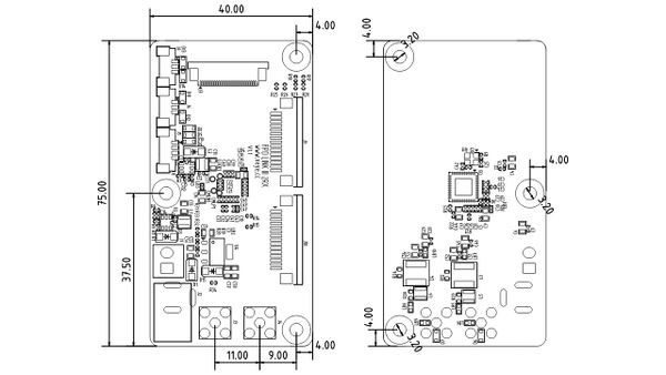
[[File:FPD-LINK3-2RX JPG DWG.jpg|alt=|none|thumb|600x600px|FPD-LINK3-2RX CAD / unit:mm]] | [[File:FPD-LINK3-2RX JPG DWG.jpg|alt=|none|thumb|600x600px|FPD-LINK3-2RX CAD / unit:mm]] | ||
[[Media:FPD-LINK3-2RX DWG.dwg|Download dwg file here]] | [[Media:FPD-LINK3-2RX DWG.dwg|Download dwg file here]] | ||
| − | + | == PCBA 3D STP File == | |
| + | [[Media:3D FPD-LINK3-2RX.zip|download 3D STP file]] | ||
Latest revision as of 02:19, 25 December 2023
FPD-LINK3-2RX Data Sheet (FPD-LINK3-2RX数据手册)
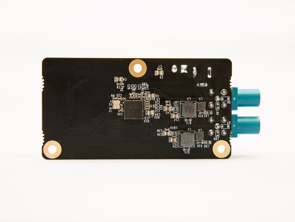
1 Product Picture(产品图片)
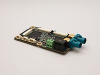
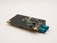
| PART NUMBER / 型号 | FRONT VIEW / 正面图片 | BACK VIEW / 背面图片 |
| FPD-LINK3-2RX |
2 Thechnical Detail (技术规格)
| Thechnical Detail (技术规格) | |
| Dual 2 MP FPD-Link III deserializer | |
| IC PART NO. | DS90UB954-Q1 / TDES954RGZT |
| Function | Deserializer |
| Input Compatibility | FPD-Link III LVDS / V3Link SerDes |
| Output Compatibility | MIPI CSI-2 |
| REFCLK | 25MHz |
| Interface | |
| MIPI Output | MIPI CSI-2 2lane ,J9 Support
MIPI CSI-2 4lane ,J7 Support |
| MIPI Output Connector | FFC socket(J7 / J9) |
| LVDS Input | FPD-Link III LVDS |
| LVDS Input Connector | FAKRA Z Compatibility * 2, J3(Port 0), J4(Port 1) |
| MPIO | Up to 7 Multi-function IO |
| Device Functional Modes | |
| FPD-Link III Operating Mode | CSI-2 Mode (DS90UB953-Q1 and DS90UB935-Q1 compatible) |
| Forward Channel Mode | Synchronous Mode |
| Back Channel Mode | Synchronous Mode |
| FPD-Link Line Rate | 4.0 Gbps |
| Back Channel Rate | 50 Mbps |
| General | |
| Operating Conditions
(Bare PCB) |
Operating guarantee temperature:-20℃~85℃, Humidity 95% or less, non-condensing |
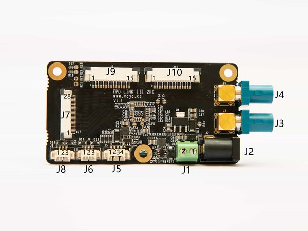
| DC Power Supply | DC 12V(J1 / J2 Input) |
| POC Power Supply | DC 9.4V(J3 / J4 Output) |
| Dimension | 75mm*40mm |
3 Board Pinlist(接口和引脚说明)
| J1:12V PWR IN(12V电源输入) | ||
| Pin NO.(引脚号) | NAME(名称) | Remarks(说明) |
| 1 | 12VIN | |
| 2 | GND | |
| J2: 12V PWR IN(12V电源输入) | |
| Connector(接插件) | Interface Definition(接口定义) |
| DC JACK | |
| J3 J4: POC interface(POC接口)
J3(Port 0 / P0) J4(Port 1 / P1) | |
| Connector(接插件) | Interface Definition(接口定义) |
| FAKRA Z | |
| J5 : RESERVE(预留未用) | ||
| Pin NO.(引脚号) | NAME(名称) | Remarks(说明) |
| 1 | MPIO4 | 3.3V LEVEL |
| 2 | MPIO5 | 3.3V LEVEL |
| 3 | MPIO6 | 3.3V LEVEL |
| 4 | GND | |
| J6 : | J8: | ||||
| Pin NO.(引脚号) | NAME(名称) | Remarks(说明) | Pin NO.(引脚号) | NAME(名称) | Remarks(说明) |
| 1 | MPIO0 | 3.3V LEVEL | 1 | MPIO2 | 3.3V LEVEL |
| 2 | GND | 2 | GND | ||
| 3 | MPIO1 | 3.3V LEVEL | 3 | MPIO3 | 3.3V LEVEL |
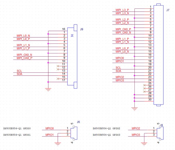
| J7: Connected to ADP-N2/N3 | ||
| Pin NO.(引脚号) | NAME(名称) | Remarks(说明) |
| 1 | GND | |
| 2 | MIPI_L3_P | |
| 3 | MIPI_L3_N | |
| 4 | GND | |
| 5 | MIPI_L2_P | |
| 6 | MIPI_L2_N | |
| 7 | GND | |
| 8 | MIPI_CK_P | |
| 9 | MIPI_CK_N | |
| 10 | GND | |
| 11 | MIPI_L1_P | |
| 12 | MIPI_L1_N | |
| 13 | GND | |
| 14 | MIPI_L0_P | |
| 15 | MIPI_L0_N | |
| 16 | GND | |
| 17 | MPIO0 | |
| 18 | MPIO1 | |
| 19 | GND | |
| 20 | SCL | 3.3V LEVEL |
| 21 | SDA | 3.3V LEVEL |
| 22 | GND | |
| 23 | MPIO2 | 3.3V LEVEL |
| 24 | MPIO3 | 3.3V LEVEL |
| 25 | NC | |
| 26 | NC | |
| 27 | NC | |
| 28 | GND | |
| J9:CSI-2 | J10:RESERVE(预留未用) | ||||
| Pin NO.(引脚号) | NAME(名称) | Remarks(说明) | Pin NO.(引脚号) | NAME(名称) | Remarks(说明) |
| 1 | GND | 1 | GND | ||
| 2 | MIPI_L0_N | 2 | MIPI_L0_N | ||
| 3 | MIPI_L0_P | 3 | MIPI_L0_P | ||
| 4 | GND | 4 | GND | ||
| 5 | MIPI_L1_N | 5 | MIPI_L1_N | ||
| 6 | MIPI_L1_P | 6 | MIPI_L1_P | ||
| 7 | GND | 7 | GND | ||
| 8 | MIPI_CK_N | 8 | MIPI_CK_N | ||
| 9 | MIPI_CK_P | 9 | MIPI_CK_P | ||
| 10 | GND | 10 | GND | ||
| 11 | NC | 11 | NC | ||
| 12 | NC | 12 | NC | ||
| 13 | SCL | 3.3V LEVEL | 13 | SCL | 3.3V LEVEL |
| 14 | SDA | 3.3V LEVEL | 14 | SDA | 3.3V LEVEL |
| 15 | NC | 15 | NC | ||
