Difference between revisions of "ADP-N1 Adapter Board Data Sheet"
Jump to navigation
Jump to search
| Line 141: | Line 141: | ||
|+J7 PIN LIST | |+J7 PIN LIST | ||
|1 | |1 | ||
| − | |||
| − | |||
| − | |||
|VCC3V3 | |VCC3V3 | ||
|POWER | |POWER | ||
|- | |- | ||
|3 | |3 | ||
| − | |||
| − | |||
| − | |||
|VCC3V3 | |VCC3V3 | ||
|POWER | |POWER | ||
|- | |- | ||
|5 | |5 | ||
| − | |||
| − | |||
| − | |||
|GND | |GND | ||
| | | | ||
|- | |- | ||
|7 | |7 | ||
| − | |||
| − | |||
| − | |||
|GND | |GND | ||
| | | | ||
| Line 171: | Line 159: | ||
|MIPI_L0_N | |MIPI_L0_N | ||
| | | | ||
| − | |||
| − | |||
| − | |||
|- | |- | ||
|11 | |11 | ||
|MIPI_L0_P | |MIPI_L0_P | ||
| | | | ||
| − | |||
| − | |||
| − | |||
|- | |- | ||
|13 | |13 | ||
|GND | |GND | ||
| | | | ||
| − | |||
| − | |||
| − | |||
|- | |- | ||
|15 | |15 | ||
|MIPI_L1_N | |MIPI_L1_N | ||
| | | | ||
| − | |||
| − | |||
| − | |||
|- | |- | ||
|17 | |17 | ||
|MIPI_L1_P | |MIPI_L1_P | ||
| | | | ||
| − | |||
| − | |||
| − | |||
|- | |- | ||
|19 | |19 | ||
|GND | |GND | ||
| | | | ||
| − | |||
| − | |||
| − | |||
|- | |- | ||
|21 | |21 | ||
|MIPI_CK_N | |MIPI_CK_N | ||
| | | | ||
| − | |||
| − | |||
| − | |||
|- | |- | ||
|23 | |23 | ||
|MIPI_CK_P | |MIPI_CK_P | ||
| | | | ||
| − | |||
| − | |||
| − | |||
|- | |- | ||
|25 | |25 | ||
| − | |||
| − | |||
| − | |||
|GND | |GND | ||
| | | | ||
|- | |- | ||
|27 | |27 | ||
| − | |||
| − | |||
| − | |||
|RESERVE | |RESERVE | ||
|Not Connected | |Not Connected | ||
|- | |- | ||
|29 | |29 | ||
| − | |||
| − | |||
| − | |||
|RESERVE | |RESERVE | ||
|Not Connected | |Not Connected | ||
|- | |- | ||
|31 | |31 | ||
| − | |||
| − | |||
| − | |||
|GND | |GND | ||
| | | | ||
|- | |- | ||
|33 | |33 | ||
| − | |||
| − | |||
| − | |||
|RESERVE | |RESERVE | ||
|Not Connected | |Not Connected | ||
|- | |- | ||
|35 | |35 | ||
| − | |||
| − | |||
| − | |||
|RESERVE | |RESERVE | ||
|Not Connected | |Not Connected | ||
| Line 269: | Line 215: | ||
|GND | |GND | ||
| | | | ||
| − | |||
| − | |||
| − | |||
|- | |- | ||
|39 | |39 | ||
|RESERVE | |RESERVE | ||
|Not Connected | |Not Connected | ||
| − | | | + | |- |
| − | | | + | | |
| − | | | + | | |
| + | | | ||
| + | |- | ||
| + | | | ||
| + | | | ||
| + | | | ||
|} | |} | ||
<nowiki>*</nowiki>Connected J5 of the VEYE-MIPI-327 camera module<br /> | <nowiki>*</nowiki>Connected J5 of the VEYE-MIPI-327 camera module<br /> | ||
==Adapter Board Dimension== | ==Adapter Board Dimension== | ||
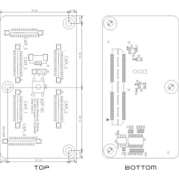
| − | [[File:ADP- | + | [[File:ADP-N1 CAD.jpg|alt=|none|thumb|600x600px|ADP-N1 CAD / unit:mm]] |
[[:File:ADP-U2-CAD.zip|Download dwg file here]] | [[:File:ADP-U2-CAD.zip|Download dwg file here]] | ||
__FORCETOC__ | __FORCETOC__ | ||
Revision as of 09:38, 14 April 2020
Adapter Board:ADP-N1 Data Sheet
1 Introduction
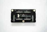
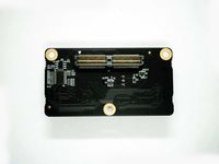
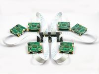
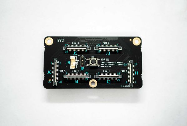
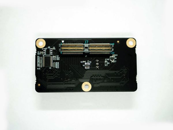
The function of ADP-U2 is to convert the interface of the VEYE-MIPI-327 camera module to the FPC28 interface of ADP-N1(a camera interposer module for AGX Xavier/TX2 DevKit).
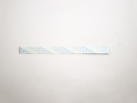
2 Product Picture
| PART NUMBER / 型号 | FRONT VIEW / 正面图片 | BACK VIEW / 背面图片 | FFC CABLE/FFC线缆 | SKETCH MAP/示意图 |
| ADP-N1 |
3 Adapter Board Pinlist
| 1 | GND | |
| 2 | RESERVE | Not Connected |
| 3 | RESERVE | Not Connected |
| 4 | GND | |
| 5 | RESERVE | Not Connected |
| 6 | RESERVE | Not Connected |
| 7 | GND | |
| 8 | MIPI_CK_P | |
| 9 | MIPI_CK_N | |
| 10 | GND | |
| 11 | MIPI_L1_P | |
| 12 | MIPI_L1_N | |
| 13 | GND | |
| 14 | MIPI_L0_P | |
| 15 | MIPI_L0_N | |
| 16 | GND | |
| 17 | IO_EXT0 | Not Connected |
| 18 | IO_EXT1 | Not Connected |
| 19 | GND | |
| 20 | SCL | 3.3V LEVEL |
| 21 | SDA | 3.3V LEVEL |
| 22 | GND | |
| 23 | IO_EXT2 | Not Connected |
| 24 | IO_EXT3 | Not Connected |
| 25 | VCC3V3 | POWER |
| 26 | VCC3V3 | POWER |
| 27 | VCC3V3 | POWER |
| 28 | GND |
| 1 | VCC3V3 | POWER |
| 3 | VCC3V3 | POWER |
| 5 | GND | |
| 7 | GND | |
| 9 | MIPI_L0_N | |
| 11 | MIPI_L0_P | |
| 13 | GND | |
| 15 | MIPI_L1_N | |
| 17 | MIPI_L1_P | |
| 19 | GND | |
| 21 | MIPI_CK_N | |
| 23 | MIPI_CK_P | |
| 25 | GND | |
| 27 | RESERVE | Not Connected |
| 29 | RESERVE | Not Connected |
| 31 | GND | |
| 33 | RESERVE | Not Connected |
| 35 | RESERVE | Not Connected |
| 37 | GND | |
| 39 | RESERVE | Not Connected |
*Connected J5 of the VEYE-MIPI-327 camera module
4 Adapter Board Dimension
