V-by-One-HS-TX
Jump to navigation
Jump to search
V-by-One-HS Data Sheet (V-by-One-HS数据手册)
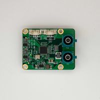
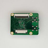
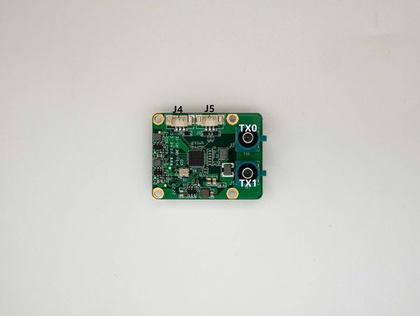
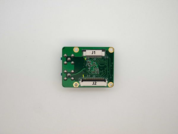
1 Product Picture(产品图片)
| PART NUMBER / 型号 | FRONT VIEW / 正面图片 | BACK VIEW / 背面图片 |
| V-by-One-HS |
2 Thechnical Detail (技术规格)
| Thechnical Detail (技术规格) | |
| V-by-One-HS serializer | |
| IC PART NO. | THCV241A-P |
| Function | Serializer |
| Input Compatibility | MIPI CSI-2 |
| Output Compatibility | V-by-One HS |
| Interface | |
| MIPI INPUT | MIPI CSI-2 4lane (800Mbsp/lane max), J1 / J2 |
| MIPI INPUT Connector | FFC socket(J1 / J2) |
| LVDS OUTPUT | V-by-One HS (3.75Gbps data rate * 2) |
| LVDS OUTPUT Connector | FAKRA Z Compatibility ( J3 / J6) |
| MPIO | 2 output,1 input |
| Device Functional Modes | |
| Clocking Mode | Synchronous Mode, FPD-Link III Clock reference derived from deserializer |
| Operating Mode | CSI-2 Mode |
| Forward Channel Mode | Synchronous Mode |
| Back Channel Mode | Synchronous Mode |
| V-by-One HS Rate | 3.75Gbps(max) * 2(Link with V-by-One-HS-RX) |
| General | |
| Operating Conditions
(Bare PCB) |
Operating guarantee temperature:-20℃~85℃, Humidity 95% or less, non-condensing |
| POC DC Power Input | DC 9-15V (J2) |
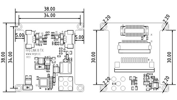
| Dimension | 29mm*37.1mm |
3 Board Pinlist(接口和引脚说明)
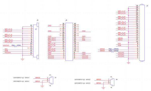
| J1:
Connect to CS-MIPI-SC132's J7 Connect to CS-MIPI-IMX307's J7 | ||
| Pin NO.(引脚号) | NAME(名称) | Remarks(说明) |
| 1 | MPIO0 | 3.3V Level |
| 2 | GND | |
| 3 | MPIO1 | 3.3V Level |
| J4 | ||
| Pin NO.(引脚号) | NAME(名称) | Remarks(说明) |
| 1 | MPIO2 | 3.3V Level |
| 2 | GND | |
| 3 | MPIO3 | 3.3V Level |
| J2:POC interface(POC接口) | |
| Connector(接插件) | Interface Definition(接口定义) |
| FAKRA Z | |
| J5 : Connect to CS-MIPI-IMX307's J8 (与CS-MIPI-IMX307 J8互联) | ||
| Pin NO.(引脚号) | NAME(名称) | Remarks(说明) |
| 1 | GND | |
| 2 | MIPI_L0_N | |
| 3 | MIPI_L0_P | |
| 4 | GND | |
| 5 | MIPI_L1_N | |
| 6 | MIPI_L1_P | |
| 7 | GND | |
| 8 | MIPI_CK_N | |
| 9 | MIPI_CK_P | |
| 10 | GND | |
| 11 | RESERVE | NC |
| 12 | RESERVE | NC |
| 13 | SCL | 3.3V Level |
| 14 | SDA | 3.3V Level |
| 15 | VCC3V3 | PWR OUT |
| J6:Connect to VEYE-MIPI-327's J5 (与VEYE-MIPI-327 J5互联) | |||||
| Pin NO.(引脚号) | NAME(名称) | Remarks(说明) | Pin NO.(引脚号) | NAME(名称) | Remarks(说明) |
| 1 | VCC3V3 | PWR OUT | 2 | VCC3V3 | PWR OUT |
| 3 | VCC3V3 | PWR OUT | 4 | VCC3V3 | PWR OUT |
| 5 | GND | 6 | GND | ||
| 7 | GND | 8 | GND | ||
| 9 | MIPI_L0_N | 10 | NC | ||
| 11 | MIPI_L0_P | 12 | NC | ||
| 13 | GND | 14 | NC | ||
| 15 | MIPI_L1_N | 16 | NC | ||
| 17 | MIPI_L1_P | 18 | NC | ||
| 19 | GND | 20 | NC | ||
| 21 | MIPI_CK_N | 22 | SDA | 3.3V LEVEL | |
| 23 | MIPI_CK_P | 24 | SCL | 3.3V LEVEL | |
| 25 | GND | 26 | GND | ||
| 27 | NC | 28 | NC | ||
| 29 | NC | 30 | NC | ||
| 31 | GND | 32 | GND | ||
| 33 | NC | 34 | NC | ||
| 35 | NC | 36 | NC | ||
| 37 | GND | 38 | NC | ||
| 39 | NC | 40 | NC | ||
| J3: RESERVE (预留) | ||
| Pin NO.(引脚号) | NAME(名称) | Remarks(说明) |
| 1 | GND | |
| 2 | VCC3V3 | PWR OUT |
| 3 | VCC3V3 | PWR OUT |
| 4 | VCC3V3 | PWR OUT |
| 5 | MPIO3 | |
| 6 | MPIO2 | |
| 7 | GND | |
| 8 | SDA | 3.3V LEVEL |
| 9 | SCL | 3.3V LEVEL |
| 10 | GND | |
| 11 | MPIO1 | 3.3V Level |
| 12 | MPIO0 | 3.3V Level |
| 13 | GND | |
| 14 | MIPI_L0_N | |
| 15 | MIPI_L0_P | |
| 16 | GND | |
| 17 | MIPI_L1_N | |
| 18 | MIPI_L1_P | |
| 19 | GND | |
| 20 | MIPI_CK_N | |
| 21 | MIPI_CK_P | |
| 22 | GND | |
| 23 | MIPI_L2_N | |
| 24 | MIPI_L2_P | |
| 25 | GND | |
| 26 | MIPI_L3_N | |
| 27 | MIPI_L3_P | |
| 28 | GND | |
