Difference between revisions of "ADP-U1 Adapter Board Data Sheet"
Jump to navigation
Jump to search
| (16 intermediate revisions by 3 users not shown) | |||
| Line 1: | Line 1: | ||
| − | |||
| − | |||
<big><big><big>'''Adapter Board:ADP-U1 Data Sheet'''</big></big></big> | <big><big><big>'''Adapter Board:ADP-U1 Data Sheet'''</big></big></big> | ||
==Introduction== | ==Introduction== | ||
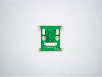
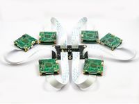
| − | The function of ADP-U1 is to convert the FPC15 interface of the CS-MIPI-IMX307 camera module to the FPC28 interface of ADP- | + | The function of ADP-U1 is to convert the FPC15 interface of the CS-MIPI-IMX307 camera module to the FPC28 interface of ADP-N1(a camera interposer module for AGX Xavier/TX2 DevKit). |
| + | |||
| + | ==Product Picture== | ||
{| class="wikitable" | {| class="wikitable" | ||
|'''PART NUMBER / 型号''' | |'''PART NUMBER / 型号''' | ||
| Line 12: | Line 12: | ||
|'''SKETCH MAP/示意图''' | |'''SKETCH MAP/示意图''' | ||
|- | |- | ||
| − | |''' | + | |'''ADP-U1''' |
|[[File:ADP-U1 001.jpg|alt=|center|thumb|200x200px|'''ADP-U1''']] | |[[File:ADP-U1 001.jpg|alt=|center|thumb|200x200px|'''ADP-U1''']] | ||
|[[File:ADP-U1 002.jpg|alt=|center|thumb|200x200px|'''ADP-U1''']] | |[[File:ADP-U1 002.jpg|alt=|center|thumb|200x200px|'''ADP-U1''']] | ||
| − | |[[File:FFC30-0.5-KH.jpg|alt=|center|thumb|200x200px|''' | + | |[[File:FFC30-0.5-KH.jpg|alt=|center|thumb|200x200px|'''FFC28P-0.5MM-20CM-T''']] |
|[[File:ADP-N1-6CAM 001.jpg|alt=|center|thumb|200x200px|'''SKETCH MAP''']] | |[[File:ADP-N1-6CAM 001.jpg|alt=|center|thumb|200x200px|'''SKETCH MAP''']] | ||
|} | |} | ||
| Line 23: | Line 23: | ||
==Adapter Board Pinlist== | ==Adapter Board Pinlist== | ||
{| class="wikitable" | {| class="wikitable" | ||
| − | | | + | | colspan="3" |'''J1 : Connect to ADP-N1''' |
| + | |- | ||
| + | |'''Pin NO.''' | ||
| + | |'''NAME''' | ||
| + | |'''Remarks''' | ||
| + | |- | ||
|1 | |1 | ||
|GND | |GND | ||
| Line 30: | Line 35: | ||
|2 | |2 | ||
|RESERVE | |RESERVE | ||
| − | | | + | |NC |
|- | |- | ||
|3 | |3 | ||
|RESERVE | |RESERVE | ||
| − | | | + | |NC |
|- | |- | ||
|4 | |4 | ||
| Line 42: | Line 47: | ||
|5 | |5 | ||
|RESERVE | |RESERVE | ||
| − | | | + | |NC |
|- | |- | ||
|6 | |6 | ||
|RESERVE | |RESERVE | ||
| − | | | + | |NC |
|- | |- | ||
|7 | |7 | ||
| Line 90: | Line 95: | ||
|17 | |17 | ||
|IO_EXT0 | |IO_EXT0 | ||
| − | | | + | |Interconnect with J3-3 (IO_EXT0) |
|- | |- | ||
|18 | |18 | ||
|IO_EXT1 | |IO_EXT1 | ||
| − | | | + | |Interconnect with J3-1 (IO_EXT1) |
|- | |- | ||
|19 | |19 | ||
| Line 114: | Line 119: | ||
|23 | |23 | ||
|IO_EXT2 | |IO_EXT2 | ||
| − | | | + | |Interconnect with J2-3 (IO_EXT2) |
|- | |- | ||
|24 | |24 | ||
|IO_EXT3 | |IO_EXT3 | ||
| − | | | + | |Interconnect with J2-1 (IO_EXT3) |
|- | |- | ||
|25 | |25 | ||
|VCC3V3 | |VCC3V3 | ||
| − | | | + | |PWR IN |
|- | |- | ||
|26 | |26 | ||
|VCC3V3 | |VCC3V3 | ||
| − | | | + | |PWR IN |
|- | |- | ||
|27 | |27 | ||
|VCC3V3 | |VCC3V3 | ||
| − | | | + | |PWR IN |
|- | |- | ||
|28 | |28 | ||
| Line 137: | Line 142: | ||
|}<br /> | |}<br /> | ||
{| class="wikitable" | {| class="wikitable" | ||
| − | | | + | | colspan="3" |'''J2 : Connect to CS-MIPI-IMX307's J7 for sync''' |
| + | |- | ||
| + | |'''Pin NO.''' | ||
| + | |'''NAME''' | ||
| + | |'''Remarks''' | ||
| + | |- | ||
|1 | |1 | ||
|IO_EXT3 | |IO_EXT3 | ||
| − | | | + | |Interconnect with J1-24 |
|- | |- | ||
|2 | |2 | ||
| Line 148: | Line 158: | ||
|3 | |3 | ||
|IO_EXT2 | |IO_EXT2 | ||
| − | | | + | |Interconnect with J1-23 |
| − | |} | + | |}<br /> |
{| class="wikitable" | {| class="wikitable" | ||
| − | | | + | | colspan="3" |'''J3:Connect to CS-MIPI-SC132's J7 for Trigger''' |
| + | |- | ||
| + | |'''Pin NO.''' | ||
| + | |'''NAME''' | ||
| + | |'''Remarks''' | ||
| + | |- | ||
|1 | |1 | ||
|IO_EXT1 | |IO_EXT1 | ||
| − | | | + | |Interconnect with J1-18 |
|- | |- | ||
|2 | |2 | ||
| Line 162: | Line 177: | ||
|3 | |3 | ||
|IO_EXT0 | |IO_EXT0 | ||
| − | | | + | |Interconnect with J1-17 |
|}<br /> | |}<br /> | ||
{| class="wikitable" | {| class="wikitable" | ||
| − | | | + | | colspan="3" |'''J4 : Connect to CS-MIPI-IMX307's J8 (Use FFC15P-1MM-5CM-Y)''' |
| + | |- | ||
| + | |'''Pin NO.''' | ||
| + | |'''NAME''' | ||
| + | |'''Remarks''' | ||
| + | |- | ||
|1 | |1 | ||
|GND | |GND | ||
| Line 208: | Line 228: | ||
|11 | |11 | ||
|RESERVE | |RESERVE | ||
| − | | | + | |NC |
|- | |- | ||
|12 | |12 | ||
|RESERVE | |RESERVE | ||
| − | | | + | |NC |
|- | |- | ||
|13 | |13 | ||
|SCL | |SCL | ||
| − | |3.3V | + | |3.3V Level |
|- | |- | ||
|14 | |14 | ||
|SDA | |SDA | ||
| − | |3.3V | + | |3.3V Level |
|- | |- | ||
|15 | |15 | ||
|VCC3V3 | |VCC3V3 | ||
| − | | | + | |PWR OUT |
| − | |} | + | |}<br /> |
==Adapter Board Dimension== | ==Adapter Board Dimension== | ||
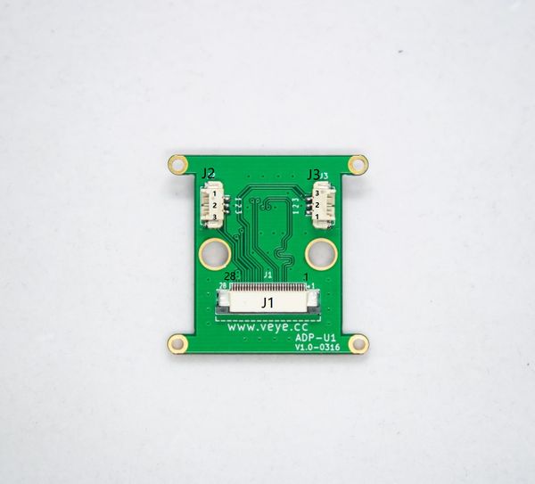
[[File:ADP-U1 CAD DRAWING.jpg|alt=|none|thumb|600x600px|ADP-U1 CAD / unit:mm]] | [[File:ADP-U1 CAD DRAWING.jpg|alt=|none|thumb|600x600px|ADP-U1 CAD / unit:mm]] | ||
| − | [[ | + | [[Media:ADP-U1-CAD.zip|Download dwg file here]] |
__FORCETOC__ | __FORCETOC__ | ||
Latest revision as of 08:41, 18 October 2021
Adapter Board:ADP-U1 Data Sheet
1 Introduction
The function of ADP-U1 is to convert the FPC15 interface of the CS-MIPI-IMX307 camera module to the FPC28 interface of ADP-N1(a camera interposer module for AGX Xavier/TX2 DevKit).
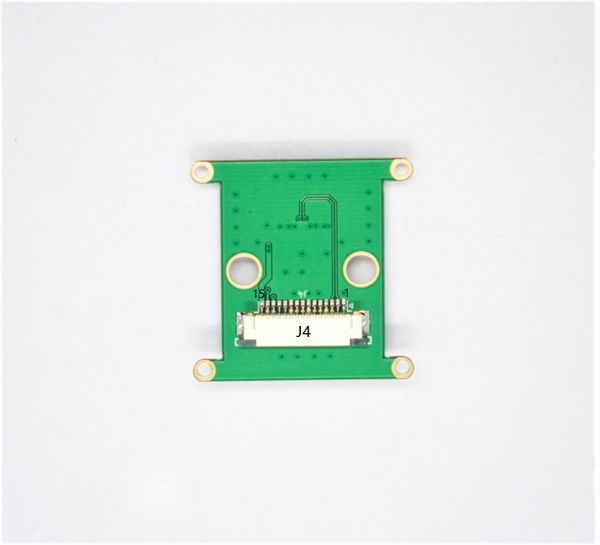
2 Product Picture
| PART NUMBER / 型号 | FRONT VIEW / 正面图片 | BACK VIEW / 背面图片 | FFC CABLE/FFC线缆 | SKETCH MAP/示意图 |
| ADP-U1 |
3 Adapter Board Pinlist
| J1 : Connect to ADP-N1 | ||
| Pin NO. | NAME | Remarks |
| 1 | GND | |
| 2 | RESERVE | NC |
| 3 | RESERVE | NC |
| 4 | GND | |
| 5 | RESERVE | NC |
| 6 | RESERVE | NC |
| 7 | GND | |
| 8 | MIPI_CK_P | |
| 9 | MIPI_CK_N | |
| 10 | GND | |
| 11 | MIPI_L1_P | |
| 12 | MIPI_L1_N | |
| 13 | GND | |
| 14 | MIPI_L0_P | |
| 15 | MIPI_L0_N | |
| 16 | GND | |
| 17 | IO_EXT0 | Interconnect with J3-3 (IO_EXT0) |
| 18 | IO_EXT1 | Interconnect with J3-1 (IO_EXT1) |
| 19 | GND | |
| 20 | SCL | 3.3V LEVEL |
| 21 | SDA | 3.3V LEVEL |
| 22 | GND | |
| 23 | IO_EXT2 | Interconnect with J2-3 (IO_EXT2) |
| 24 | IO_EXT3 | Interconnect with J2-1 (IO_EXT3) |
| 25 | VCC3V3 | PWR IN |
| 26 | VCC3V3 | PWR IN |
| 27 | VCC3V3 | PWR IN |
| 28 | GND | |
| J2 : Connect to CS-MIPI-IMX307's J7 for sync | ||
| Pin NO. | NAME | Remarks |
| 1 | IO_EXT3 | Interconnect with J1-24 |
| 2 | GND | |
| 3 | IO_EXT2 | Interconnect with J1-23 |
| J3:Connect to CS-MIPI-SC132's J7 for Trigger | ||
| Pin NO. | NAME | Remarks |
| 1 | IO_EXT1 | Interconnect with J1-18 |
| 2 | GND | |
| 3 | IO_EXT0 | Interconnect with J1-17 |
| J4 : Connect to CS-MIPI-IMX307's J8 (Use FFC15P-1MM-5CM-Y) | ||
| Pin NO. | NAME | Remarks |
| 1 | GND | |
| 2 | MIPI_L0_N | |
| 3 | MIPI_L0_P | |
| 4 | GND | |
| 5 | MIPI_L1_N | |
| 6 | MIPI_L1_P | |
| 7 | GND | |
| 8 | MIPI_CK_N | |
| 9 | MIPI_CK_P | |
| 10 | GND | |
| 11 | RESERVE | NC |
| 12 | RESERVE | NC |
| 13 | SCL | 3.3V Level |
| 14 | SDA | 3.3V Level |
| 15 | VCC3V3 | PWR OUT |
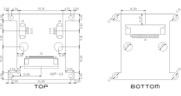
4 Adapter Board Dimension
